- 您现在的位置:买卖IC网 > Sheet目录3818 > PIC18F4620-I/ML (Microchip Technology)IC MCU FLASH 32KX16 44QFN
2001 Microchip Technology Inc.
Advance Information
DS39541A-page 293
PIC18C601/801
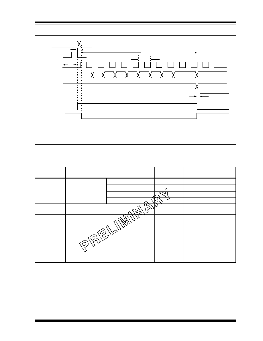
FIGURE 22-23:
A/D CONVERSION TIMING
TABLE 22-23: A/D CONVERSION REQUIREMENTS
Param
No.
Symbol
Characteristic
Min
Max
Units
Conditions
130
TAD
A/D clock period
PIC18C601/801
1.6
20(5)
sTOSC based, VREF ≥ 3.0V
PIC18LC601/801
3.0
20(5)
sTOSC based, VREF full range
PIC18C601/801
2.0
6.0
sA/D RC mode
PIC18LC601/801
3.0
9.0
sA/D RC mode
131
TCNV
Conversion time
(not including acquisition time)(1)
11
12
TAD
132
TACQ
Acquisition time(3)
15
10
—
s
-40
°C ≤ Temp ≤ 125°C
0
°C ≤ Temp ≤ 125°C
135
TSWC
Switching time from convert
→ sample
—
(Note 4)
136
TAMP
Amplifier settling time(2)
1
—
s
This may be used if the “new”
input voltage has not
changed by more than 1 LSb
(i.e., 5 mV @ 5.12V) from the
last sampled voltage (as
stated on CHOLD).
Note 1: ADRES register may be read on the following TCY cycle.
2: See Section 17.0 for minimum conditions, when input voltage has changed more than 1 LSb.
3: The time for the holding capacitor to acquire the “New” input voltage, when the voltage changes full scale
after the conversion (AVDD to AVSS, or AVSS to AVDD). The source impedance (RS) on the input channels is
50
.
4: On the next Q4 cycle of the device clock.
5: The time of the A/D clock period is dependent on the device frequency and the TAD clock divider.
131
130
132
BSF ADCON0, GO
Q4
A/D CLK
A/D DATA
ADRES
ADIF
GO
SAMPLE
OLD_DATA
SAMPLING STOPPED
DONE
NEW_DATA
(Note 2)
98
7
2
1
0
Note
1:
If the A/D clock source is selected as RC, a time of TCY is added before the A/D clock starts.This allows the
SLEEP
instruction to be executed.
2: This is a minimal RC delay (typically 100 ns), which also disconnects the holding capacitor from the analog input.
. . .
TCY
发布紧急采购,3分钟左右您将得到回复。
相关PDF资料
PIC24HJ256GP210-I/PT
IC PIC MCU FLASH 128KX16 100TQFP
PIC24HJ128GP310A-I/PF
IC PIC MCU FLASH 128KB 100-TQFP
DSPIC33FJ128GP310-I/PF
IC DSPIC MCU/DSP 128K 100TQFP
PIC16C66-20I/SO
IC MCU OTP 8KX14 PWM 28SOIC
DSPIC33FJ128MC510-I/PT
IC DSPIC MCU/DSP 128K 100TQFP
PIC16C66-20I/SP
IC MCU OTP 8KX14 PWM 28DIP
PIC18LF2620-I/SP
IC MCU FLASH 32KX16 28SDIP
PIC16F877-04I/P
IC MCU FLASH 8KX14 EE 40DIP
相关代理商/技术参数
PIC18F4620-I/P
功能描述:8位微控制器 -MCU 64KB 3968 RAM 36 I/O RoHS:否 制造商:Silicon Labs 核心:8051 处理器系列:C8051F39x 数据总线宽度:8 bit 最大时钟频率:50 MHz 程序存储器大小:16 KB 数据 RAM 大小:1 KB 片上 ADC:Yes 工作电源电压:1.8 V to 3.6 V 工作温度范围:- 40 C to + 105 C 封装 / 箱体:QFN-20 安装风格:SMD/SMT
PIC18F4620-I/P
制造商:Microchip Technology Inc 功能描述:IC 8BIT FLASH MCU 18F4620 DIP40
PIC18F4620-I/PT
功能描述:8位微控制器 -MCU 64KB 3968 RAM 36 I/O RoHS:否 制造商:Silicon Labs 核心:8051 处理器系列:C8051F39x 数据总线宽度:8 bit 最大时钟频率:50 MHz 程序存储器大小:16 KB 数据 RAM 大小:1 KB 片上 ADC:Yes 工作电源电压:1.8 V to 3.6 V 工作温度范围:- 40 C to + 105 C 封装 / 箱体:QFN-20 安装风格:SMD/SMT
PIC18F4620-I/PT
制造商:Microchip Technology Inc 功能描述:IC 8BIT FLASH MCU 18F4620 TQFP44
PIC18F4620T-I/ML
功能描述:8位微控制器 -MCU 64KB 3968 RAM 36 I/O RoHS:否 制造商:Silicon Labs 核心:8051 处理器系列:C8051F39x 数据总线宽度:8 bit 最大时钟频率:50 MHz 程序存储器大小:16 KB 数据 RAM 大小:1 KB 片上 ADC:Yes 工作电源电压:1.8 V to 3.6 V 工作温度范围:- 40 C to + 105 C 封装 / 箱体:QFN-20 安装风格:SMD/SMT
PIC18F4620T-I/PT
功能描述:8位微控制器 -MCU 64KB 3968 RAM 36 I/O RoHS:否 制造商:Silicon Labs 核心:8051 处理器系列:C8051F39x 数据总线宽度:8 bit 最大时钟频率:50 MHz 程序存储器大小:16 KB 数据 RAM 大小:1 KB 片上 ADC:Yes 工作电源电压:1.8 V to 3.6 V 工作温度范围:- 40 C to + 105 C 封装 / 箱体:QFN-20 安装风格:SMD/SMT
PIC18F4680-E/ML
功能描述:8位微控制器 -MCU 64KB 3328 RAM w/ECAN RoHS:否 制造商:Silicon Labs 核心:8051 处理器系列:C8051F39x 数据总线宽度:8 bit 最大时钟频率:50 MHz 程序存储器大小:16 KB 数据 RAM 大小:1 KB 片上 ADC:Yes 工作电源电压:1.8 V to 3.6 V 工作温度范围:- 40 C to + 105 C 封装 / 箱体:QFN-20 安装风格:SMD/SMT
PIC18F4680-E/P
功能描述:8位微控制器 -MCU 64KB 3328 RAM w/ECAN RoHS:否 制造商:Silicon Labs 核心:8051 处理器系列:C8051F39x 数据总线宽度:8 bit 最大时钟频率:50 MHz 程序存储器大小:16 KB 数据 RAM 大小:1 KB 片上 ADC:Yes 工作电源电压:1.8 V to 3.6 V 工作温度范围:- 40 C to + 105 C 封装 / 箱体:QFN-20 安装风格:SMD/SMT